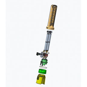
We can make 3D output according to the customer's samples data, and make 2D mold layout drawings and 3D mold design drawings.
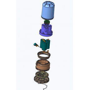
Make 2D mold layout drawings and 3D mold design drawings.
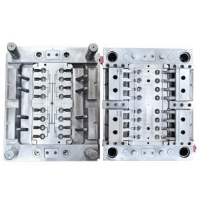
Mold Design & Engineering Injection mold design is a crucial element of the injection molding process, as it plays a significant role in determining the quality and accuracy of the final product. The process involves creating molds for plastic materials that are precisely engineered to create the exact shape and size of the product required. The design process can involve several stages, beginning with a concept phase where basic ideas and sketches are explored, followed by detailed planning and engineering to finalize the design. We can make 3D output according to the customer's samples data, and make 2D mold layout drawings and 3D mold design drawings.
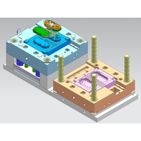
Mold Design & Engineering Injection mold design is a crucial element of the injection molding process, as it plays a significant role in determining the quality and accuracy of the final product. The process involves creating molds for plastic materials that are precisely engineered to create the exact shape and size of the product required. The design process can involve several stages, beginning with a concept phase where basic ideas and sketches are explored, followed by detailed planning and engineering to finalize the design. We can make 3D output according to the customer's samples data, and make 2D mold layout drawings and 3D mold design drawings.
.png)
PCB redesign. djt-e has done all optimizations and modifications djt-e could until the present moment. The current prototype (last picture) needs more hardware and firmware tests, maybe some further modifications in the project of the PCB, then can produce a batch of 100pcs for extensive tests and pre-compliance/EMC tests. If this project reaches expectations and goals, for me it will be like a small dream come true. Sirros IoT SX project. PCB: 10cm x 9cm, 1.6mm thickness, 8 layers PCB Stack: L1: Top L2: GND plane L3: Power plane L4: Signals L5: GND plane L6: Signals L7: GND plane L8: Bottom Blind vias: (vias that begin in an external layer and end on an inner layer) - L1 to L2 - L1 to L4 - L8 to L4 The light green circles surround signal vias that when they make the transition of the routing layer they change the ground reference plane. For all signal vias in which occurs this, there is a GND stitching via very close, to shorten the path of the return currents of the signal...
.png)
djt-e is committed to being a professional and trustworthy partner in Electronics manufacturing service(EMS), including turnkey electronic assembly and materials management services, to original equipment manufacturers (OEMs) in the electronics industry. Below are our major business: 1. PCB, Flex-Rigid PCB, PCB Assembly, PCB Fabrication and PCB Layout from concept to volume manufacturing 2. Wire Assembly and Cable Harness 3. Box-building and Injection molding 4. Focus on Provide High Reliability Electronic Manufacturing Service SMT / PCBA / OEM / EMS 5. membrance switch,Rubber keypad …
.png)
PCB design process In electronic design and development, attention should be paid to PCB design and electronic component selection. 1. PCB design shall consider wiring, SMT difficulty, separation of analog circuit and digital circuit, electromagnetic interference between components and circuits and other related issues. Pay special attention to the problem of interference, because such problems are sometimes hidden problems, which may appear at some time. It would be embarrassing if it appeared after large-scale production. 2. For the problem of component selection, the use of side door should be avoided in the selection of electronic components, because this component may face shutdown at any time or be difficult to be compatible with other components. Sometimes replacing a component will cause great trouble because the pin pin pin or drive is incompatible. For products, the use of mature and stable components can not only improve the stability of products, but also sometimes reduce ...
.png)
Our primary business is contract manufacturing for PCBAs in southern China, and although we do have customers throughout the world, but do not currently stock materials or finished product anywhere but China. Lead times vary, and really have to do with the complexity of the product and the components used. As I'm sure you know, components are the driver for lead-times on finished product in the current post pandemic world. If you do have customers that would need PCBA production services while taking advantage of the lower cost capability of China manufacturing, we would certainly be interested in the opportunity to quote the project. In addition, we can help with design services for new concepts, reverse engineering, product redesigns, etc. These engineering services are provided both locally in the USA and in China. We can also offer mechanical design as well, if there is a need for your customer.
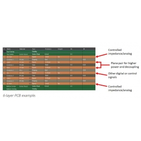
How to Route Signals Before you start routing, let’s look at the typical PCB stackup you would use in a 6-layer PCB: In this stackup, the top and bottom layers are on thin dielectrics, so these layers should be used for impedance controlled signals. 10 mil is probably the thickest dielectric you should use because this will require microstrip routing with 15-20 mil width, depending on dielectric constant. If you’re routing a digital interface with differential pairs, the spacing will also allow a reduced trace width, which will allow you to route into finer pitch components. Just as an example, we have used a version of the above stackup for many of our small form factor networking products that support multiple multi-gigabit Ethernet channels. If you need to use much smaller trace widths on the outer layers, just decrease the outer dielectric thicknesses (maybe as low as 4-5 mil), and then add some thickness to the L3-L4 dielectric so that you hit your board thicknes...
.png)
According to your ideas or design requirements, we can put your ideas throughout the whole design process, from concept to product, through the establishment of design specifications, create information to build the original function board, and further improve the design to complete the required products. This includes creating schematics, PCB layouts, mechanical drawings, bill of materials, and assembly and test procedures and specifications& nbsp;< br />Software and hardware < br / >We have in-house expertise in writing software for embedded controllers and user interfaces for PCs, tablets and smartphones< br />Function hand board < br / >We have a complete manufacturing and all electronic parts suppliers, so that we can produce the required functional hand board, submit customer requirements for testing and evaluation< br />Specific design capabilities are as follows < br / >• Simulation design < br / >• Digital design < br / >• RF and microwave design < br / >&bul...
.png)
How to test the PCBA board? 1. PCBA board manual test Manual testing is to test directly by the vision and confirm the component mounting on PCB through vision and comparison. This technology is widely used. However, the large number and small components make this method more and more unsuitable. Moreover, some functional defects are not easy to be found, and the data is not easy to collect. In this way, more professional testing methods are needed. 2. PCBA board automatic optical inspection (AOI) Automatic optical testing, also known as automatic visual testing, is carried out by a special tester. It is used before and after reflow and has a good effect on the polarity inspection of components. Easy-to-follow diagnosis is a common method, but this method is poor in short circuit identification. 3. PCBA board flying needle tester Needle testing has been widely welcomed in the past few years due to advances in mechanical accuracy, speed, and reliability. In addition, the requirements f...
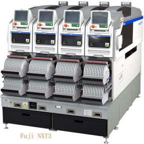
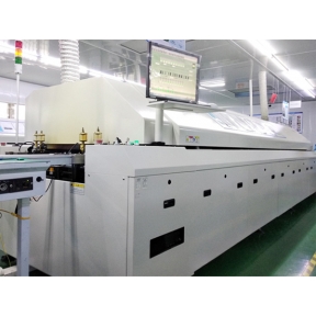
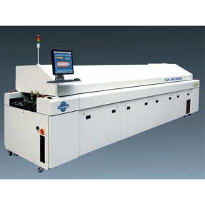
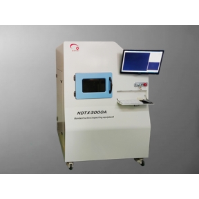
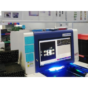
Printed Circuit Board Assembly Overview 100% 3D X-ray Inspection after SMT and at Final QA on every leadless part to ensure no shorts, opens, or voids are present Content 100% Inline AOI ensures no errors with parts placement, mis-alignment, mis-orientation, and solder joint defects 12 zone ovens with on-demand Liquid Nitrogen for 99.99% purity on solder joints Dual wave and Selective wave Soldering Machines 100% Inline Solder Paste Inspection First article QA Inspection done on every job Flying Probe Test Parametric Bench Test
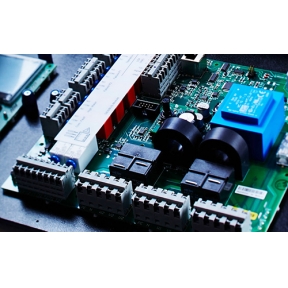
EMS (electronics manufacturing services) electronic manufacturing is a service process that makes product design concept into product. It needs to integrate electronic technology, supply chain, engineering process, production management and human resources, and has high professionalism. We provide customers with one-stop EMS electronic manufacturing services, including design, component procurement, PCB manufacturing, placement, plug-in, testing, assembly and other processes. DesignCustomers generally provide product design scheme, including schematic diagram, drawings, layout, MCU program, BOM, PCB gerbers, assembly SOP and other documents. We can also provide joint development services for customers, build prototypes according to product concepts, and then determine technical parameters, product structure and development cycle, so as to rapidly promote R & D and mass production. Sample prototypeAccording to the design scheme, we can quickly make mold shell, PCB circuit boar...
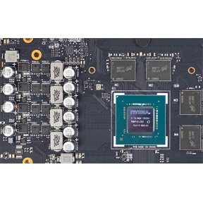
Rapid proofing of PCBWe are extremely good at providing customers with the shortest 24 hours of fast circuit board proofing service. When your company needs fast circuit board proofing, you only need to deliver the documents to us, you can receive high-quality circuit boards in a very short time, and have a very attractive price competitiveness. In addition, we will also reflect the design problems found in your PCB proofing process in the trial production report. All DFM manufacturability inspection and process problem finding reports are free of charge. Many PCB rapid proofing companies in the market put together more than a dozen boards for cutting production, which will lead to a lot of quality problems. We only produce each PCB separately to ensure the quality, so as to reduce the accuracy of PCB circuit simulation verification. PCB multilayer board and complex technologySupport 1 to 36 layers of multilayer board, HDI, blind hole, BGA, pan hole, gold finger, resin plug hole, ...
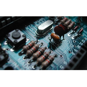
Why outsourcing electronic components procurement?With the refinement of industrial division of labor, more and more electronic product R & D companies streamline organizational structure, allocate limited resources in the two core competitiveness of R & D and sales, so as to outsource the cumbersome production and manufacturing links. In this trend, it is bound to increase the demand for PCBA labor and materials. Customers only need to provide design documents for electronic manufacturers to purchase electronic components and complete the PCBA manufacturing process according to the design requirements. This mode of labor and material contracting can save the staff cost and dull cost of customers' self built materials purchasing, inspection and warehousing. On the whole, it will save the total cost of customers' enterprises and improve the financial and product turnover efficiency. How can we ensure that the electronic components procurement is a genuine channel?We have a perfect ...
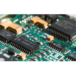
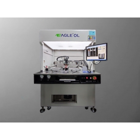
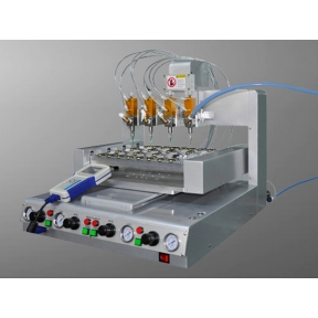
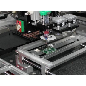
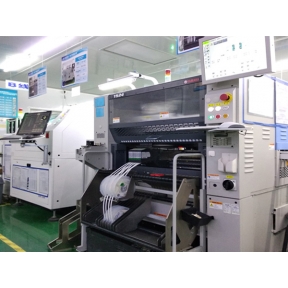
we provide customers with high-end SMT chip processing services, equipped with four automatic high-speed SMT chip production lines, automatic loading machine, automatic solder paste printing machine, SPI solder paste thickness detector, multi temperature zone reflow soldering, AOI optical testing equipment, X-ray inspection machine, baking machine, steel mesh cleaning machine, etc., and provide processing and manufacturing services for domestic listed companies and group customers for a long time. The company has passed iso9001:2015 quality management system, ISO13485 medical device management system, iatf16949 automotive electronic certification, etc., supporting the mounting of 0201 components, 0.4mm pitch BGA, QFN and other precision electronic components. Our SMT chip processing advantages1) More than 15 quality team members, effectively control IQC incoming inspection, IPQC process inspection, OQA delivery inspection and other important process links;2) Equipped with a team ...
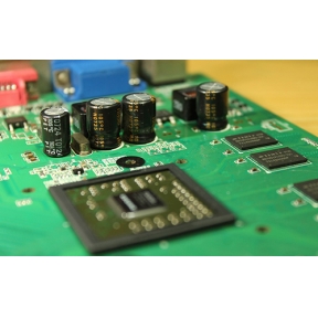
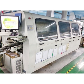
Process capability of dip plug-in processingAOI of plug-in is used to detect the error, leakage and inversion of components, and strictly control the dip through rateThe skilled soldering hand with strict training can control the welding speed and qualityAccording to the status of the circuit board, the temporary storage area with independent identification around the pull wire: to be inserted, to be repaired, to be inspected by QC, defective products, to be inspected by QA, etc., to avoid mixed boardStrict IPQC and QA lot sampling standards to ensure the reliability of DIP processing Dip plug in processing equipmentPlug in line x 2Plug in AOI: check the bad items of plug-in components and solder jointsWave soldering x 2 setsRear welding stay wire x 24 stationWashing machine x 1 set Dip plug-in processing is a part of PCBA electronic processing process. There are more manual operations, which puts forward higher requirements for management. Through the implementation of a set...
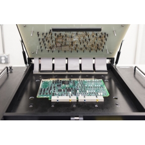
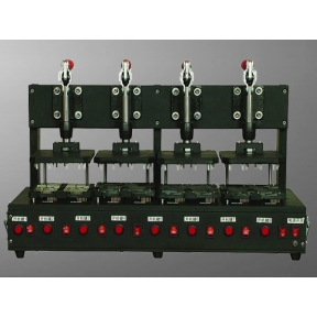
PCBA test (English PCBA test) refers to the electrical conductivity of PCBA circuit board mounted with electronic components and the test based on input and output values. In the design of PCB circuit board, there is a numerical relationship between different test points, such as voltage and current. It needs to use professional test equipment or manual operation multimeter to test the test points, so as to verify whether the actual PCBA Board meets the design requirements. PCBA test is the key step to ensure the quality of production and delivery. According to the test points, procedures and test steps designed by customers, FCT test fixture is made, and then PCBA board is placed on FCT test rack to complete the test< br /> PCBA testing principleConnect the test points on PCBA board through FCT test rack to form a complete channel, connect the computer and the burner, and upload the MCU program. MCU program will capture the user's input action (for example, long press the switch ...
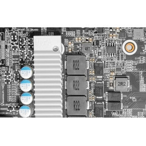
Engineering Technology PCB circuit board manufacturing and PCBA processing technology has developed for nearly 100 years. From the initial thin film technology to the present advanced automatic circuit printing and mounting technology, it has witnessed the efforts and technological leaps of countless industry predecessors. The trend of miniaturization in the semiconductor industry also promotes the rapid development of PCB industry technology. Nowadays, it is common to produce more than 20 layers of PCB and mount 01005 package components. Our team of engineers spend a lot of energy, in line with the purpose of serving the industry entry-level and high-level applications, and start to edit and organize this engineering technology learning garden, so as to truly realize the & lt; A site clearance industry;. Printed circuit board (PCB) is based on the circuit design of electronic products, which is made by a technology similar to circuit printing. It is used to carry components ...

100% 3D X-ray Inspection after SMT and at Final QA on every leadless part to ensure no shorts, opens, or voids are present Content 100% Inline AOI ensures no errors with parts placement, mis-alignment, mis-orientation, and solder joint defects 12 zone ovens with on-demand Liquid Nitrogen for 99.99% purity on solder joints Dual wave and Selective wave Soldering Machines 100% Inline Solder Paste Inspection First article QA Inspection done on every job Flying Probe Test Parametric Bench Test
Mobile:13326856492 Telephone:0755-84827607
Email:[email protected]