Engineering Technology
PCB circuit board manufacturing and PCBA processing technology has developed for nearly 100 years. From the initial thin film technology to the present advanced automatic circuit printing and mounting technology, it has witnessed the efforts and technological leaps of countless industry predecessors. The trend of miniaturization in the semiconductor industry also promotes the rapid development of PCB industry technology. Nowadays, it is common to produce more than 20 layers of PCB and mount 01005 package components. Our team of engineers spend a lot of energy, in line with the purpose of serving the industry entry-level and high-level applications, and start to edit and organize this engineering technology learning garden, so as to truly realize the & lt; A site clearance industry;.
Printed circuit board (PCB) is based on the circuit design of electronic products, which is made by a technology similar to circuit printing. It is used to carry components such as integrated circuit (IC), resistor, capacitor, led and so on. From this, a PCB containing components (PCB + assembly) is formed, That is the electronic hardware of the product. In general, the designer has to write a software program and burn it into the core IC to & lt; Hardware + software & quot; To realize the design principle of electronic circuit and I / O control, similar to our current computer host + windows system to realize various complex I / O operations. Assembly in PCBA includes a series of processes such as SMT chip processing, dip plug-in processing, PCBA testing (ICT / FCT testing), etc< br />
PCB history
Looking back on the development history of PCB in the early 20th century: the first batch of PCB patents; Printed wire & quot; It was released in the early 20th century, but the industry recognized that PCB was first put into use after the Second World War. In 1925, Charles middot of the United States; Charles Ducas filed a patent application, proposing a method of using conductive ink to form an electrical path directly on the insulating surface through template printing. Paul middot, Austrian scientist; Dr. Eisler invented the first operational printed circuit board in 1943.
1920s
The earliest printed circuit board (PCB) was made of bakelite, wood-based panel, laminated paperboard and even veneer. Drill holes in the material and place the flat Brass & lt; Wire & quot; Riveted or bolted to the plate. The connection to the part is usually achieved by pressing the end of the brass mark on the blind rivet, while the lead of the part is simply pressed into the open end of the rivet. Occasionally small nuts and bolts are used instead of rivets. This form of circuit board was used in early tube radios and gramophone products.
1950s-1960s
Laminates made from a mixture of different types of resins and materials were introduced, but PCBs were still single-sided. The circuit board and components are on different sides. Compared with the bulky wiring and cable, the advantage of PCB makes it the first choice for new products to enter the market. But the biggest impact on the development of printed circuit board comes from the government agencies responsible for developing new weapons and communication equipment. They use wire end components in some applications. After the lead wires of components are placed through holes, they are fixed on the board with small nickel plates welded on the lead wires.
Late 1960s
The production process of printed circuit board has undergone a huge evolution, and finally developed the process of copper plating on the borehole wall. This allows the circuits on both sides of the board to be electrically connected. Copper has replaced brass as the preferred metal because of its current carrying capacity, relatively low cost and ease of manufacture. In 1956, the U.S. Patent Office issued a & lt; Circuit assembly process & quot; A small group of scientists, represented by the US Army, applied for the patent. The patented process involves the use of a substrate (such as melamine), laminating copper foil and depicting the circuit diagram, and then taking photos to imitate the offset plate. Etch one side of the acid resistant ink printed on the copper foil to remove the exposed copper, leaving & lt; Printing line & quot;. The die is then used to punch holes in the drawing to match the location of the component wires or terminals. The lead wire is passed through the non electroplated hole in the laminate, and then the card is immersed or floated on the molten solder groove. The solder covers the weld bead and connects the leads of the component to the weld bead. This is the rudiment of PCB technology.
Since 1980s
With the rapid development of PCB technology, PCB technology has evolved from single-layer board to multi-layer board, from 6mil line width to 3mil line distance. Gradually able to produce high precision and high frequency requirements of the circuit board, such as HDI, blind hole and other processes. Moreover, the development of the whole printed circuit board industry is also highly automated. With the introduction of various precision exposure machines, etching and electroplating equipment, PCB can be more miniaturized and miniaturized to meet the requirements of the current electronic products era.
The history of PCB is also the history of semiconductor. At present, 5nm process is coming soon, which means that we can concentrate more complex products on smaller PCBs. Since 1925, the development of PCB has become mature, and the manufacturing process of the industry is relatively perfect. Even the FPC flexible printed circuit board (FPC) and rigid flex printed circuit board (FPC FPC FPC FPC FPC FPC FPC FPC FPC FPC FPC FPC FPC FPC FPC FPC FPC FPC FPC FPC FPC FPC FPC FPC FPC FPC FPC FPC FPC FPC FPC FPC FPC FPC FPC FPC FPC. The history of PCB is a history of technological transition, which has witnessed the efforts and efforts of countless people in the industry< br />
Difference between PCB and PCBA
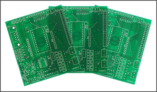
PCB is the abbreviation of printed circuit board, commonly known in the industry as & lt; Bare board& ldquo; Base plate;, That is, there are no components on the surface. PCBA is the abbreviation of PCB + assembly, which refers to a board with OK hardware function formed by welding electronic components (such as IC, resistor, capacitor, inductor, led, crystal oscillator, etc.) to PCB bare board. A bit similar to the construction industry, PCB is the foundation, PCBA is the whole building after the construction on the foundation. The figure below more intuitively explains the image difference between PCB and PCBA< br />
.png)
PCB classification
PCB is the basic component of electronic products. For products with different uses, different PCBs need to be selected. Usually, we will classify PCBs by the number of layers, base material and scope of application.
1. According to the number of PCB layers to distinguish, generally divided into: single panel, double-sided board and multilayer board.
Single panel is to concentrate all the components on one side of the PCB board, so it is called single panel. Because the area of single panel is limited, the circuit design will be relatively simple, which is only applicable to the electronic products with simple functions.
Double sided PCB refers to that both sides of PCB have components and circuits. Under the same size, it will double the design area of single panel. It can effectively solve the electromagnetic interference problem caused by wire interleaving in single panel and reduce the product volume. It can be used in products with complex circuit design.
Multilayer board is composed of single panel and double-sided board. The most common method is to use two double-layer boards as the inner board, and then two single-layer boards as the outer side. Through the positioning system and insulating adhesive material, the multilayer board is composed of four layers. Of course, the number of layers can be increased according to the design scheme of the product, which is generally even. The design of multilayer board improves the area and density of wiring, and can do more complex circuit design. The components of multilayer board are more chip type components, and the layout of components is more precise, so the product can be lighter and smaller.

2. According to the nature of PCB, it can be divided into rigid circuit board, flexible circuit board, soft and hard combination board.
The main materials of rigid circuit board are FR-4, CEM-1, CEM-3 and metal based copper clad laminate (mainly aluminum based, a few iron-based).
FR-4 is a glass fiber board made of copper foil and impregnated flame retardant epoxy fiber cloth, which has good machinability.
CEM-1 is a composite substrate made of paper material with glass fiber on the upper and lower surfaces and phenolic resin in the middle. Its machinability and electrical properties are not as strong as FR-4, but its price is cheap.
CEM-3 is a composite fiberglass board. The glass transition temperature, resistance to immersion welding, peel strength, water absorption, electric breakdown, insulation resistance and UL index have reached the level of FR-4. But the bending strength is lower than that of FR-4.
Metal based copper clad laminate is composed of metal substrate, insulating medium layer and conductive layer (generally copper foil) by hot pressing. The most important feature of metal based copper clad laminate is its excellent heat dissipation performance and dimensional stability.
Generally, rigid circuit board is used in electronic products. Rigid circuit board has a certain mechanical strength, and PCB has flatness, which can maintain a good overall state.
Flexible circuit boards are mostly made of soft laminated plastics such as polyester film, polyimide film and ethylene fluoride propylene film. The flexible circuit boards can be bent and retracted to facilitate special installation according to installation requirements.
The combination of hard and soft PCB is the combination of rigid pcb and flexible PCB to form a PCB with FPC characteristics and PCB characteristics. It can be used in some products with special requirements.
3. According to the scope of application, PCB can be divided into high frequency and low frequency.
High frequency of electronic products is the current development trend. PCB high-frequency board has been widely used in the communication industry, network technology and high-speed information processing system. Because the dielectric constant of high-frequency board is small, the heating efficiency and signal transmission speed of high-frequency board are very fast. At the same time, the material of high-frequency board has low water absorptionSo it can be used in more humid environment. The application range is much larger than the low frequency board.


.png)
